
Why Semiconductor Fabs Are Switching to Titanium: Applications in Wet Etch, CVD, and Ultra-Pure Fluid Systems
A technical overview of titanium's growing role in semiconductor manufacturing — covering wet etch baths, CVD chamber components, ultra-pure water systems, and CMP slurry delivery, with grade selection data and contamination control requirements specific to fab environments.
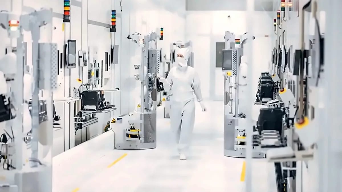
The semiconductor industry operates at the intersection of extreme chemical aggression and extreme cleanliness. Process chemistries include hydrofluoric acid, nitric acid, sulfuric acid, hydrogen peroxide, and ammonia — often at elevated temperatures and in sequences that cycle between oxidizing and reducing conditions. The materials that contain and deliver these chemistries must resist corrosion without leaching metallic contaminants that would kill device yield. Titanium meets both requirements in ways that stainless steel, fluoropolymers, and even some exotic alloys cannot.
Where Titanium Is Used in the Fab
Wet Etch and Clean Stations
Wet etch processes use hot acid baths to selectively remove material from wafer surfaces. The most demanding chemistry is the SC-1 clean (APM: ammonium hydroxide + hydrogen peroxide + water) followed by SC-2 (HPM: hydrochloric acid + hydrogen peroxide + water), typically at 60–80 °C. Grade 2 titanium resists both chemistries with negligible corrosion rates, while 316L stainless steel pits in hot HCl-peroxide mixtures and releases iron, chromium, and nickel ions that contaminate wafer surfaces.
Components: Bath tanks, overflow weirs, heater housings, drain fittings, circulation piping Grade: Grade 2 (ASTM B265 plate, ASTM B338 tube) Surface finish: Electropolished to Ra < 0.25 μm, passivated to minimize particle shedding
CVD and PVD Chamber Components
Chemical vapor deposition (CVD) and physical vapor deposition (PVD) processes operate at temperatures from 200 °C to over 600 °C in reactive gas environments including titanium tetrachloride, silane, tungsten hexafluoride, and plasma-activated species. Titanium is used for chamber liners, shower heads, gas distribution rings, and substrate heater assemblies where its combination of temperature resistance, chemical inertness, and low outgassing rate provides advantages over aluminum and stainless steel.
Components: Chamber liners, gas distribution plates, electrode rings, heater enclosures Grade: Grade 2 for temperatures below 300 °C; Grade 5 for structural components at higher temperatures Key property: Low outgassing rate prevents process contamination from material off-gassing
Ultra-Pure Water (UPW) Systems
Semiconductor-grade ultra-pure water (18.2 MΩ·cm resistivity, < 1 ppb total metals) is used in enormous quantities for wafer rinsing between process steps. The distribution piping, valves, and fittings that deliver UPW must not contribute metallic contamination. Grade 2 titanium piping maintains UPW quality over decades of service without the periodic replacement that PVDF (polyvinylidene fluoride) plastic piping requires due to degradation from ozone-treated water.
Components: Distribution headers, branch lines, valve bodies, sampling ports Grade: Grade 2 seamless tube per ASTM B338 Advantage: Unlike PVDF, titanium does not degrade under UV-ozone treatment used for biofilm control in UPW loops
CMP Slurry Delivery
Chemical mechanical planarization (CMP) uses abrasive slurries containing silica, alumina, or ceria nanoparticles in acidic or alkaline carriers. The delivery piping and pump components must resist the combined erosion-corrosion of abrasive particles in corrosive fluids. Titanium's hard passive oxide film resists erosion significantly better than stainless steel, extending component life by 3–5 times in slurry delivery applications.
Components: Slurry distribution manifolds, valve bodies, pump housings Grade: Grade 5 for pump impellers (higher hardness), Grade 2 for piping
Contamination Control Requirements
Semiconductor applications impose contamination requirements far beyond those of industrial chemical processing:
| Parameter | Industrial Standard | Semiconductor Requirement |
|---|---|---|
| Surface finish (Ra) | < 1.6 μm | < 0.25 μm (electropolished) |
| Surface metallic ions | Not specified | < 10 atoms/cm² per element |
| Particle count | Not specified | < 50 particles > 0.2 μm per cm² |
| Passivation | Standard acid passivation | Electropolish + citric acid passivation + UPW rinse |
| Packaging | Standard wrapping | Double-bagged in cleanroom, nitrogen purge |
| Handling | Standard gloves | Class 100 cleanroom gloves, no skin contact |
Meeting these requirements adds cost — typically 30–50 percent over industrial-grade titanium components — but is non-negotiable for fab applications where a single contamination event can scrap hundreds of wafers worth tens of thousands of dollars.
Grade Selection for Semiconductor
| Application | Recommended Grade | Why |
|---|---|---|
| Wet etch baths | Grade 2 | Corrosion resistance in acid mixtures, formability for tank fabrication |
| UPW piping | Grade 2 | Corrosion resistance, weldability, standard availability |
| CVD chamber components | Grade 2 or Grade 5 | Temperature resistance; Grade 5 for structural loads |
| CMP pump impellers | Grade 5 | Higher hardness resists erosive wear |
| Gas delivery fittings | Grade 2 | Corrosion resistance in halogen gas environments |
| Heater assemblies | Grade 5 | Elevated temperature strength retention |
Why the Semiconductor Industry Is Growing Titanium Demand
Three trends are accelerating titanium adoption in semiconductor manufacturing:
Advanced node migration. As transistor dimensions shrink below 3 nm, contamination budgets tighten proportionally. Materials that were acceptable at 14 nm — including some grades of stainless steel — are being replaced with titanium at 3 nm and below because their leaching rates exceed the tighter metal ion specifications.
Fab expansion. The global wave of semiconductor fab construction — over USD 200 billion in announced investments through 2028 — is creating demand for titanium piping, tanks, and components in quantities the titanium industry has not previously seen from this sector.
Sustainability requirements. Titanium's 40+ year service life in corrosive fab environments aligns with the semiconductor industry's sustainability targets. Replacing PVDF piping every 5–7 years and fluoropolymer-lined tanks every 10 years generates significant plastic waste that titanium eliminates.
BAOTI Semiconductor-Grade Titanium
BAOTI supplies Grade 2 and Grade 5 titanium in tube, plate, bar, and custom machined components for semiconductor fab applications. We provide electropolished surfaces to Ra < 0.25 μm, cleanroom packaging, and full material certification including metallic ion surface analysis documentation. Contact our semiconductor applications team for specifications and lead times.
Frequently Asked Questions
Why is titanium used in semiconductor manufacturing?
Titanium resists the aggressive acid chemistries used in semiconductor wet etch and cleaning processes (HF, HCl, H₂SO₄, H₂O₂) without leaching metallic contaminants that would reduce device yield. Its corrosion resistance, low outgassing, and ultra-clean surface finish make it superior to stainless steel in fab environments.
What titanium grade is used in semiconductor fabs?
Grade 2 commercially pure titanium is the standard for wet etch baths, ultra-pure water piping, and gas delivery fittings. Grade 5 (Ti-6Al-4V) is used for CVD chamber components and CMP pump impellers where higher strength, hardness, or temperature resistance is needed.
What surface finish is required for semiconductor-grade titanium?
Semiconductor applications require electropolished surfaces to Ra < 0.25 μm, surface metallic ions below 10 atoms/cm² per element, and particle counts below 50 particles >0.2 μm per cm². Components must be passivated with citric acid, rinsed with UPW, and double-bagged in cleanroom conditions.
How does titanium compare to PVDF in semiconductor UPW systems?
Titanium UPW piping lasts 40+ years without degradation, while PVDF plastic piping requires replacement every 5–7 years due to degradation from ozone-treated water. Titanium also resists UV-ozone biofilm treatment and does not generate plastic waste, aligning with fab sustainability goals.
Why is semiconductor demand for titanium growing?
Three factors drive growth: advanced node migration below 3 nm requiring tighter contamination control (replacing stainless steel with titanium), a global wave of over USD 200 billion in new fab construction, and sustainability targets that favor titanium's 40+ year service life over disposable polymer alternatives.
Related Reading

Titanium Pressure Vessels, Reactors, and Condensers: Design Standards and Solid vs. Clad Economics
An engineering and procurement guide to titanium chemical processing equipment — covering ASME Section VIII design rules, solid vs. explosion-clad construction crossover thickness, grade selection for corrosive media, and 30-year lifecycle cost comparisons.

Sourcing Custom Titanium Machined Parts: Tolerances, Surface Finishes, and OEM Ordering Guide
A practical procurement guide for buyers ordering custom CNC-machined titanium parts — covering achievable ISO 2768 tolerances, surface finish specifications, near-net forging vs. bar-stock machining economics, and incoming quality inspection checklists.

Titanium in Oil and Gas: Where It Outperforms Super Duplex and Nickel Alloys
An application-focused guide to titanium in upstream and downstream oil and gas — covering subsea risers, heat exchangers, downhole tools, and desulfurization equipment, with grade selection data and real-world case studies showing where titanium displaces super duplex stainless steel and nickel alloys.

Titanium vs Aluminum: When to Upgrade and When Aluminum Is Good Enough
A practical engineering comparison of titanium and aluminum alloys — covering strength-to-weight ratio, corrosion resistance, temperature limits, cost per part, and decision criteria for aerospace, marine, chemical, and medical applications.